Soundcard Interface
 In my day job I have access to top-of-the-line test equipment, but I can't very well bring all my home projects to work to test there.
I therefore need to set up a compact audio analyser system at home using a laptop and soundcard, and one of the many free analyser software packages you can get.
But a soundcard is fragile; feed in too much voltage and it is toast. And valve amplifiers have a lot of voltage.
I therefore decided to build an interface box to go between the DUT and the soundcard.
This project is havily based on (plagiarised from!) Pete Millet's Soundcard Interface.
I pretty much copied his design, with some changes to make it more compact since I wanted it to fit on a 100x100mm PCB or less.
I also made some feature changes to suit my needs better.
In my day job I have access to top-of-the-line test equipment, but I can't very well bring all my home projects to work to test there.
I therefore need to set up a compact audio analyser system at home using a laptop and soundcard, and one of the many free analyser software packages you can get.
But a soundcard is fragile; feed in too much voltage and it is toast. And valve amplifiers have a lot of voltage.
I therefore decided to build an interface box to go between the DUT and the soundcard.
This project is havily based on (plagiarised from!) Pete Millet's Soundcard Interface.
I pretty much copied his design, with some changes to make it more compact since I wanted it to fit on a 100x100mm PCB or less.
I also made some feature changes to suit my needs better.
Overview
All inputs and outputs are fully balanced.
The output of the DUT is fed through high-voltage blocking capacitors, to the input attenuator.
This has 100k input impedance and offers three attenuation options: x1, x10, x100.
There is also the option to ground one side for unbalanced signals, which is how it will be used most of the time.
The signal is then buffered and unbalanced to scrub away any common-mode interference.
Then it is re-balanced and sent out to the soundcard at a safe level.
The generator signal path provides gain for the ordinarily-small soundcard generator signal level, to make it more useful, and can also drive lower-impedace loads than the soundcard itself can.
The output can be grounded on one side if necessary.
There is a peak voltmeter which can monitor the signal level being sent to the DUT from the generator (GEN), or the signal being sent to the soundcard (DUT).
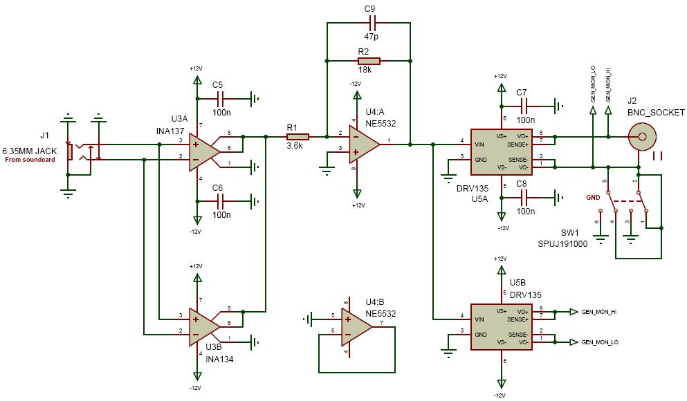
Input Attenuator
The signal first passes through high-voltage DC blocking caps C15 & C16.
R12 & R13 ensure they can discharge after switch off, otherwise you might get an unpleasant surprise when plugging a different amplifier into the interface later...
Everything else forms the balanced attenuator.
I didn't want to use a large rotary switch for the attenuator; I used small push-button switches for everything.
SW2 can be used to ground one 'leg' of the signal, for monitoring unbalanced signals.
Strictly speaking, SW2 might see high voltages that my little PCB switches are not rated for, but I'm willing to let it suffer occasionally. Naughty naughty!
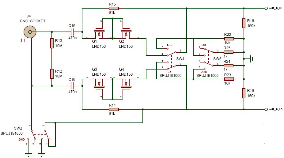
In the x1 position as shown, the signal passes through Q1/2/3/4, which are LND150 depletion MOSFETs.
The purpose of these MOSFETs is to limit the fault current into the interface if too much voltage is applied, but without adding excessive Johnson noise.
For small signals they look like a resistance equal Rds(on), which is only about 3k in each leg of the circuit, but under overload conditions the fault current will be limited to the MOSFETs' Idss of a few milliamps.
This means input voltages up to about 500Vpk can be tolerated without blowing anything up, but without adding significant noise.
This was a major shortcoming of Pete's circuit, in my opinion, as he used a simple 50k series protection resistance, which added considerable Johnson noise and (more importantly) common-mode distortion.
R18 and R19 are the opamp bias resistances, and in parallel with the opamp's own input impedance create roughly 100k total input impedance.
Pushing the 'attn' button switches the signal away from the MOSFETs and puts R14 & R15 (91k) in series with each leg.
Simultaneously, this also switches in a different shunt resistance, formed by R22/23/24/25, which is selectable between 10k or 1k with the other button, giving either x10 or x100 attenuation.
Originally I also included a loop-back button like on Pete's interface, which fed the generator signal back into the DUT path so it could be monitored.
However, this caused way too much crosstalk between the generator output and the DUT path owing to switch capacitance, which would have made distortion measurements above about 1kHz unreliable.
I strongly suspect Pete's interface will suffer the same problem, unreported.
DUT Signal Path
D2/3/4/5 are protection diodes that feed a pair of 10V Zener diodes, D6 & D7.
Input voltages larger than 10.6V peak will be clamped, safely protecting the opamp, and the fault current through these diodes is limited by the LND150s or R14/15, depending on the setting of the attenuator.
The purpose of D8/9/16/17 is to cancel out the common-mode distortion that would otherwise be introduced by the protection diodes' nonlinear junction capacitance.
Remember the effective resistance of the LND150s was about 3k, so by making R3 & R5 equal to this, each input pin of the opamp sees a matching 3k source impedance and a pair of diodes.
This symmetry eliminates the common-mode distortion.
R4 can be included to provide gain, but currently I do not have it fitted so this part of the circuit is unity gain.
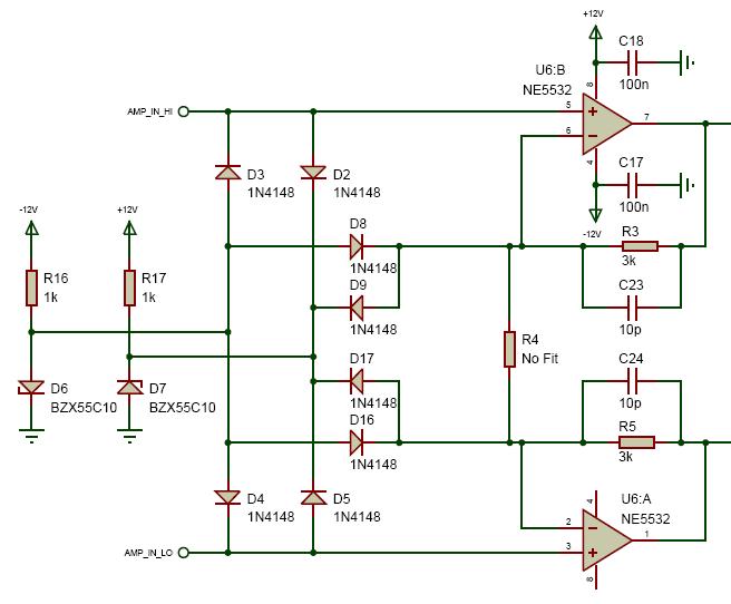
The buffered signal is then fed into a differential amplifier U9 -actually two differential amplifiers in parallel!
The reason for doing this is because I didn't want to share one dual opamp between the DUT path and the generator path because it would probably cause crosstalk, so I was faced with the possibility of a spare opamp in both signal paths.
I therefore decided to build two differential amps in parallel, since this theoretically improves the noise figure of this circuit section by 3dB.
As built, it doesn't really make any difference to the overall noise performance of the interface since the input buffers dominate, but one day I may experiment with different opamps.
In any case, I've never used parallel diff amps before, and this was a good excuse to try it.

The unbalanced signal from the diff amp then feeds a peak-detection circuit, and the output driver U7.
U7 is a DRV135 which balances the signal and sends it to the soundcard via the 1/4" jack J5.
I made provision for using a SMD or DIP device which is why you see two on the schematic; only one is actually fitted.
Notice R20 & R21 which drop the voltages to U7's supply pins.
These are unusually large, which deliberately reduces the supply voltages to U7.
This is a safety featutre -it inherently limits the output voltage to less than about 5Vpp from either output, which should keep the soundcard safe from overdrive.
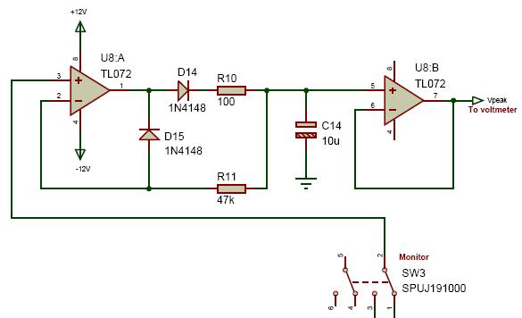
Peak Voltmeter
Pete's project has a true-RMS, autoranging meter built in, which adds quite a lot to the cost and complexity of his interface.
I decided to go for something a lot simpler.
I mostly work with peak voltages, not RMS, and in any case I expect the analyser software to be capable of giving me an RMS conversion.
It is of course easy to calculate the RMS value of a sine or trangle wave from its peak value, and non-ideal signals I would probably be monitoring on an oscilloscope anyway, which can also do RMS measurement.
I therefore chose to include a simple peak-reading voltmeter, using one of those ultra-cheap 3-wire voltmeter modules you can buy on eBay.
The output of the generator path or the DUT path -selected by the monitor switch sW3- is sent to a precision rectifier built around U8A.
The DC voltage stored on C14 is equal to the peak voltage of the signal, and is buffered by U8B which drives the voltmeter.
Generator Signal Path
The generator signal path is simple.
It's main purpose is to amplify the test signal produced by the sound card, to get a more-useful level for testing amplifiers.
The signal from the soundcard is buffered and unbalanced by U3, which is an INA137 (again, I made provision for SMD and DIP packages, so you see two on the schematic but only one is fitted).
U4 then provides gain of x5, but you could chage this gain by adjusting R1 and R2 to suit your requirements.
In future I might hack the design to put a level pot here.
Note that U4 is an inverting amp because this avoids adding common-mode distortion, but the input jack J1 has its balanced connections swapped, so overall the signal path is noninverting.
Finally, U5 re-balances the signal (SMD or DIP) and the amplified test signal is available from the BNC connector J2.
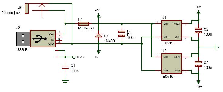
Power Supply
The power supply is extremely simple.
5V power can come from USB or a 5V adapter, the same as on Pete's project.
Power first passes through a resettable fuse F1 before going to a pair of isolating DC-DC switching converters U1 & U2, which generate the two 15V bipolar power rails.
They're labelled 12V because I originally also used 12V linear regulators,
but they made no significant difference to the final audio performance so I stayed with 15V to get more output from the generator.
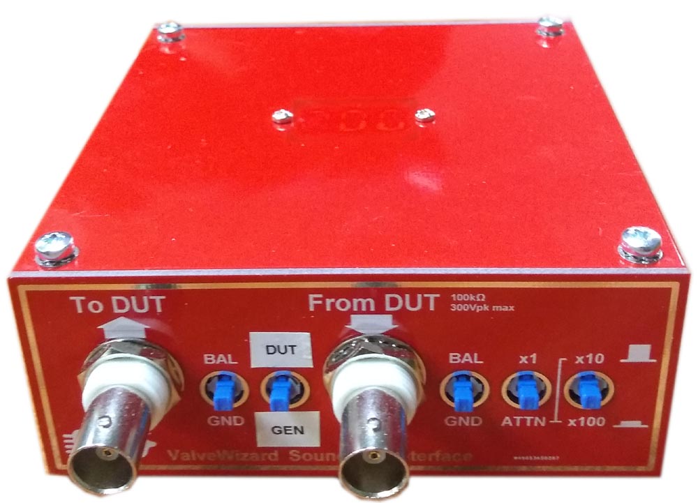
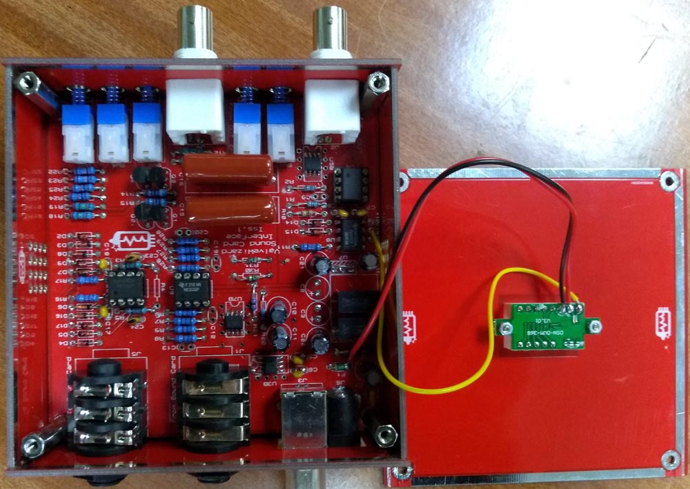
Enclosure
The enclosure itself is also built from PCB material. This is a great way to make a shielded box complete with professional-looking silkscreen.
It's a idea I picked up from this Hackaday article.
Performance
It is not possible to measure the distortion floor of this project by analog means because it is below the noise floor.
Whatever it is, it is below 0.01% under all practical conditions, which is plenty good enough.
Full schematic here.
If you want to build it yourself, here are the Gerber files (700kB).
|